What a keypad has to do
A silicone keypad does three things at once: it gives the user a defined force and travel, it provides the snap that tells the finger the key has actuated, and it carries a conductive pill that closes a circuit on the PCB underneath. Each of those is set by a different part of the design, and confusing them is why keypads that feel right fail electrically or vice versa.
The force and the snap come from the web, the thin membrane that connects each key to its neighbours. The electrical contact comes from the carbon pill on the underside of the key and the track geometry on the board. The travel is the gap between the two, set by the moulding and by the assembly.
A keypad is therefore a mechanical spring and an electrical switch in one moulded part, and the two have to be designed together. A web that gives a pleasant 2 N actuation with 0.6 mm travel leaves very little margin for a board that is not perfectly flat.
The web sets the force
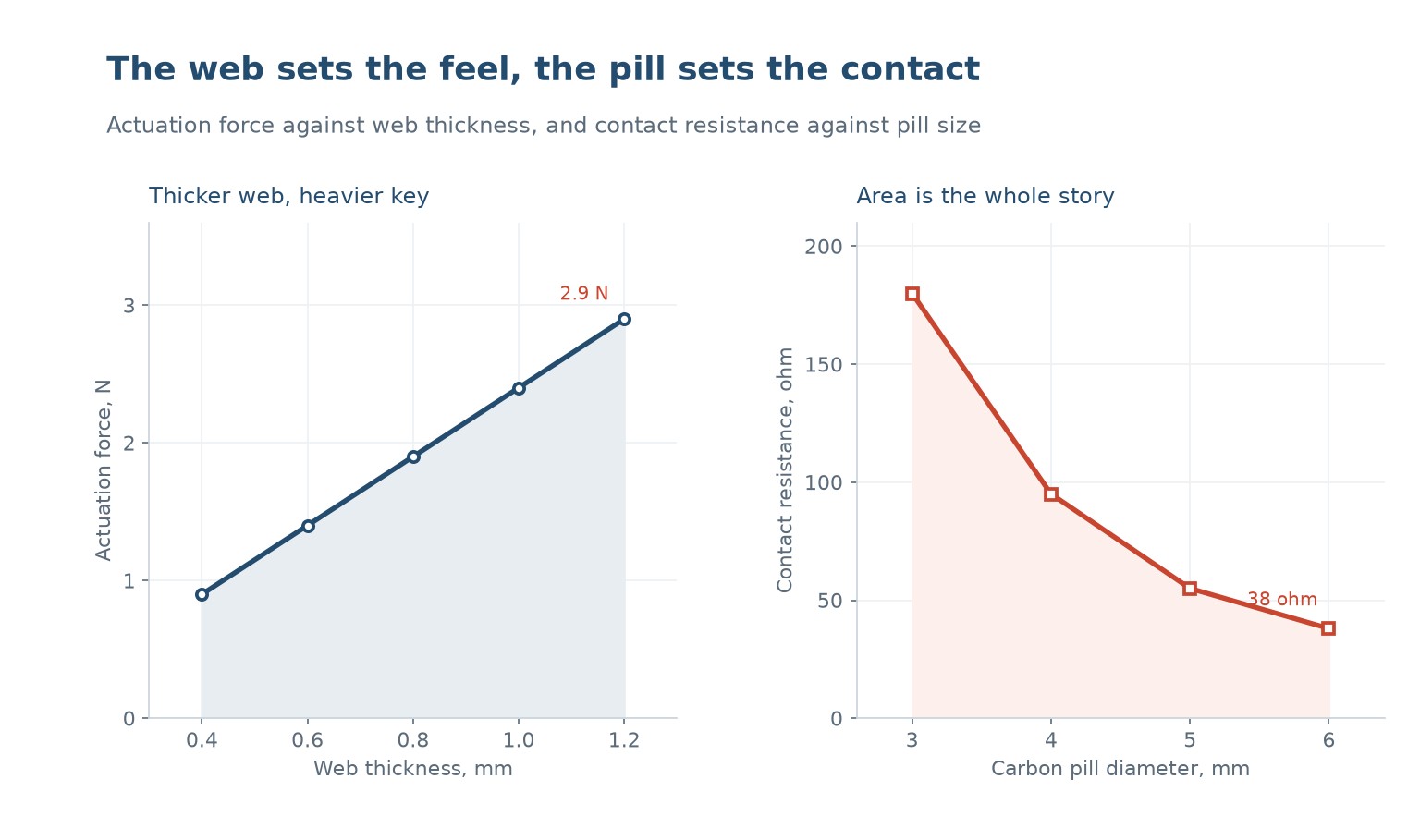
Actuation force is dominated by the web thickness and the web geometry, not by the compound hardness. A 0.4 mm web actuates at about 0.9 N; a 1.2 mm web actuates at about 2.9 N. That is a factor of three from a thickness change, and it is the lever a designer actually has.
Hardness matters far less than most people expect. Moving from 40 to 60 Shore A changes the actuation force by perhaps 10 to 15 percent on the same web, because the force is dominated by the bending stiffness of a thin membrane, and bending stiffness scales with the cube of thickness and only linearly with modulus. Thickness wins.
That is also why a keypad cannot be tuned by changing compound at the last minute. If the force is wrong, the tool has to change. The only process lever is the moulding temperature, which changes the modulus slightly and the residual stress more, and neither is a substitute for the right web.
Travel and the snap ratio
The snap is a buckling event. As the key is pressed the web deflects, the force rises to a peak, and then the web buckles and the force drops. The ratio of peak force to the force after buckling is the snap ratio, and it is what the finger feels as a click. A snap ratio below about 1.4 feels mushy; above about 2.0 feels sharp and is hard to press evenly.
The snap ratio depends on the web's shape as much as its thickness. A domed web buckles more sharply than a flat one, and a web with a small radius at the key edge buckles more sharply than one with a large radius. This is why two keypads with the same actuation force can feel completely different.
Travel is set by the gap between the pill and the board, not by the web. A web can deflect 1 mm while the pill only has 0.3 mm to travel, and in that case the key bottoms out on the board before the web buckles, which removes the snap entirely. Getting the travel right is a stack-up problem, and it is where most keypad complaints originate.
| Web thickness | Actuation force | What it suits |
|---|---|---|
| 0.4 mm | 0.9 N | Light touch, handheld, high key count |
| 0.6 mm | 1.4 N | General consumer devices |
| 0.8 mm | 1.9 N | Industrial panels, gloved use |
| 1.0 mm | 2.4 N | Heavy duty, deliberate actuation |
| 1.2 mm | 2.9 N | Very stiff, check the user can press it repeatedly |
Table 1 — Web thickness against actuation force
The carbon pill and contact resistance
The pill is a disc of carbon-loaded silicone, moulded into the key or inserted afterwards. Its job is to bridge two tracks on the board, and the resistance of that bridge depends mostly on its area: a 3 mm pill gives about 180 ohm, a 6 mm pill about 38.
That resistance is in series with the board's own track resistance and the contact resistance at the pill surface, and it matters because most keypad circuits are scanned with a low current. A 180 ohm pill in a matrix that expects 50 ohm can read as a missed key, especially as the pill ages and its surface oxidises.
Pill flatness matters more than pill size past a point. A large pill that is domed will only touch on its rim, and the contact area collapses to a ring rather than a disc. That is why pill moulding tolerance and the flatness of the key underside are specified together, and why a pill that looks generous can still read high.
| Pill diameter | Typical resistance | Opmerkingen |
|---|---|---|
| 3 mm | 180 ohm | Marginal for low-current scan circuits |
| 4 mm | 95 ohm | Acceptable for most consumer boards |
| 5 mm | 55 ohm | Comfortable margin |
| 6 mm | 38 ohm | Generous, but check the key footprint |
Table 2 — Carbon pill size against contact resistance
Moulding the web without thin spots
The web is the thinnest feature in the part and the hardest to fill. Silicone is shear-thinning but still viscous, and a 0.4 mm web across a wide span is a long flow path with a large pressure drop. The result is a web that is thinner in the middle of the span than at the key, which changes the force of the keys in the middle of the array.
The fix is usually a combination of a hotter mould, a slower injection and a gate position that feeds the web from the edge rather than through the keys. A hot mould reduces viscosity; a slow injection avoids shear heating that cures the compound early; an edge gate lets the web fill before the keys, which is the opposite of what a metal mould designer would do.
Venting matters too, because the web is a large thin area and air has to leave it. A web that traps air shows as a milky patch, which is cosmetic on a black keypad and a functional defect on a translucent one.
Testing a keypad
The first test is force and travel on a press with a load cell, on a sample of keys across the array, not on one key in the middle. The middle keys are the ones with the longest web flow path and the thinnest web, so they are the ones that will be out of specification.
The second is contact resistance, measured through the actual scan circuit rather than with a multimeter on the pill. A pill that reads 50 ohm on a bench meter can read 300 ohm in a circuit that only supplies 10 microamps, because the contact is not fully wetted at low current.
The third is life. A keypad is a fatigue component, and the web cracks at the key edge after a number of cycles that depends on the strain at that edge. A web that is too thin for the travel will fail early, and the failure looks like a tear at the corner of a key rather than a wear-out of the pill.
Can the actuation force be adjusted after the tool is made?
Only slightly, by changing the mould temperature or by adding a shim under the key. Neither is a real adjustment. If the force is outside the target, the web has to change, which means a tool change or a tool insert.
Why do the middle keys feel different from the edge keys?
Because the web flow path is longer, so the web is thinner in the middle of the array. The fix is a gate position or a runner design that equalises the fill, not a change in compound.
What causes a keypad to fail electrically but still feel fine?
Usually the pill. A domed pill, an oxidised surface or a pill that is too small for the scan current will read high or intermittently while the mechanical feel is unchanged. Contact resistance measured in the real circuit is the only reliable test.
Is laser etching of the key legends reliable?
It is, if the key surface is moulded flat and the compound is consistent. Etching removes material, so it also changes the surface finish locally, and on a backlit keypad the etched area has to be translucent enough to pass light.
How much travel should a key have?
Typically 0.25 to 0.5 mm for a consumer key and up to 1 mm for an industrial one, but the number that matters is the travel before the pill touches the board. If the web bottoms out first, the snap disappears regardless of the nominal travel.
Can silicone keypads be overmoulded onto a plastic frame?
Yes, and it is common on automotive and industrial panels. The bond depends on the frame material and on a mechanical interlock, because silicone does not adhere to most thermoplastics without a primer.
A keypad that feels right but reads wrong?
Send the keypad drawing with the web section, the pill size and the board track layout. We will tell you where the force and the contact resistance are likely to land.
Continue reading
- Silicone Compression Moulding: Pressure, Cure and the Flash Line
- Silicone Injection Molding: Cold Runner, LSR and the Metering Unit
- Silicone Mould Design: Shrinkage, Draft and Where the Part Sticks
- Silicone Hardness: What Shore A Actually Tells You
- Custom Silicone Rubber: Moulding, Tooling and Tolerances



 NL
 EN
 ES
 FR
 DE
 PT
 AR
 RU
 JA
 KO
 IT
 TR
 PL
 ID